 |
|
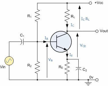
The Common Emitter Amplifier In the Transistor tutorial we saw that the most common circuit configuration for a transistor is that of the Common Emitter Amplifier and that a family of curves known commonly as the Output Characteristics Curves, relates the Collector current (Ic), to the output or Collector voltage (Vce), for different values of Base current (Ib) signal. All types of signal amplifiers operate using AC signal inputs which alternate between a positive value and a negative value so some way of presetting the amplifier circuit to operate between these two maximum or peak values is required. This is achieved using a process known as Biasing. Biasing is very important in amplifier design as it establishes the correct operating point of the amplifier thereby reducing any distortion to the input signal. We also saw that a DC load line can be drawn onto these output characteristics curves to show all the possible operating points from fully "ON" to fully "OFF" of the transistor and to which the Quiescent Point or Q-point can be found. The aim of any small signal amplifier is to amplify all of the input signal with the minimum distortion possible to the output, in other words, the output signal must be an exact reproduction of the input signal but only bigger (amplified). To obtain low distortion when used as an amplifier the operating quiescent point needs to be correctly selected. This is in fact the DC operating point of the amplifier and its position may be established at any point along the load line by a suitable biasing arrangement. The best possible position for this quiescent point is as close to the centre position of the load line as reasonably possible, thereby producing a Class A type amplifier operation, ie. Vce = 1/2Vcc. Consider the Common Emitter Amplifier circuit shown below. The Common Emitter Amplifier Circuit
The quiescent Base voltage (Vb) is determined by the potential divider network formed by the resistors, R1 and R2 and the power supply voltage Vcc and this is given as:
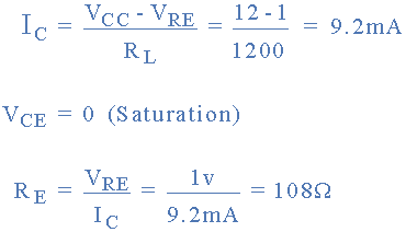
This same supply voltage also determines the Collector current, Ic when the transistor is fully "ON" (saturation), Vce = 0. The Base current Ib for the transistor is found from the Collector current, Ic and the DC current gain Beta, ß of the transistor. For example, assume a load resistor, RL of 1.2kOs and a supply voltage of 12v. Calculate the Collector current (Ic) flowing through the load resistor when the transistor is switched fully "ON", assume Vce = 0. Also find the value of the Emitter resistor, Re with a voltage drop of 1v across it.
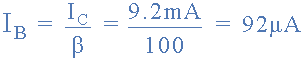
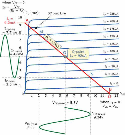
This then establishes point "A" on the Collector current vertical axis of the characteristics curves and occurs when Vce = 0. When the transistor is switched fully "OFF", their is no voltage drop across either resistor Re or RL as no current is flowing through them. Then the voltage drop across the transistor, Vce is equal to the supply voltage, Vcc. This then establishes point "B" on the horizontal axis of the characteristics curves. Generally, the Q-point of the amplifier is half-way along the load line so the Collector current will be given as half of 9.2mA. Therefore Q = 4.6mA. This DC load line produces a straight line equation whose slope is given as: -1/(RL + Re) and that it crosses the vertical Ic axis at a point equal to Vcc/(RL + Re). The actual position of the Q-point on the DC load line is determined by the mean value of Ib. As the Collector current of the transistor, Ic is also equal to the DC gain Beta, times the Base current (ß x Ib), if we assume a Beta (ß) value for the transistor of say 100, the Base current Ib flowing into the transistor will be given as:
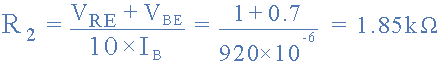
Resistors, R1 and R2 are chosen to give a quiescent Base current of 92uA. The current flowing through the potential divider circuit has to be large compared to the actual Base current, Ib, so assume a value of 10 times Ib flowing through the resistor R2. This then gives the value of R2 as:
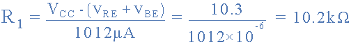
If the current flowing through resistor R2 is 10 times the value of the Base current, then the current flowing through resistor R1 must be 11 times the value of the Base current at 1012uA or 1mA. The voltage across resistor R1 is equal to Vcc - 1.7v (Vre + 0.7 for silicon transistor) which equals 10.3V, therefore R1 is given as:
So, for our example above, the preferred values of the resistors chosen to give a tolerance of 5% (E24) are:
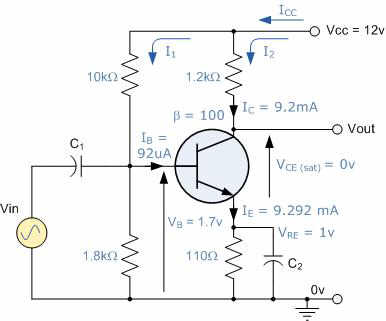
Then, our original Common Emitter circuit above can be rewritten to include the values of the components that we have just calculated. Completed Common Emitter Circuit
In common emitter amplifier circuits, capacitors C1 and C2 are used as Coupling Capacitors to ensure that the bias condition set up for the circuit to operate correctly is not effected by any additional external circuits or components connected to the amplifier, as the capacitors will only pass AC signals and block any DC component. So far, so good. We can now draw the load line onto the curves for the load resistor RL of 1.2kO. When the transistor is switched "OFF", Vce equals the supply voltage Vcc and this is point B on the line. Likewise when the transistor is fully "ON" and saturated the Collector current is determined by the load resistor, RL and this is point A on the line. We calculated before from the DC gain of the transistor that the Base current required for the mean position of the transistor was 92uA and this is point Q on the load line which is also the Quiescent point or Q-point of the amplifier. We could quite easily make life easy for ourselves and round off this value to 100uA exactly, without any effect to the operating point. Output Characteristics Curves
Point Q on the load line gives us the Base current operating point of Ib = 92uA. We need to find the maximum and minimum peak swings of Base current that will result in a proportional change to the Collector current, Ic without any distortion to the input signal. As the load line cuts through equal spacings of the DC characteristics curves we can find the peak swings of Base current equally spaced along the load line, and these are points N and M on the line, giving a minimum and maximum Base current of 25uA and 175uA respectively. Any input signal giving a Base current greater than these values will cause the transistor to go beyond point N and into its Cut-off region or beyond point M and into its Saturation region thereby resulting in distortion to the signal. Using points N and M, the instantaneous values of Collector current and corresponding values of Collector-emitter voltage can be projected from the load line. It can be seen that the Collector-emitter voltage is in anti-phase (-1800) with the collector current. As the Base current Ib changes in a positive direction from 92uA to 175uA, the Collector-emitter voltage, which is also the output voltage decreases from its steady state value of 5.8v to 2.0v. Therefore, a single stage Common Emitter Amplifier is also an Inverting Amplifier. So, for our simple example above we can now summarise all the values calculated for our simple common emitter amplifier circuit as:
|
|
|
|
Contact email: qooljaq@qooljaq.com |