 |
|
Basic function Class C is defined as an anode conduction angle of less than 180 degrees. In Class C, the amplifying device is deliberately not operated linearly. Instead, it is operated as a switch in order to reduce resistance loss. The anode conduction angle in Class C operation is usually made as short as is possible. In effect, the tank circuit makes the RF output sine wave--like a bell that is struck at a constant rate by a hammer. This is similar to the principal behind the spark transmitter. The efficiency of a typical Class C amplifier is high. When compared to a Class AB1 or Class AB2 amplifier operating at the same power input, a Class C amplifier will deliver a received signal increase of about 1db--in other words, 1/6 of 1 S-unit. However, significant trade-offs are required to achieve that 1/6 of 1 S-unit. As is the case with Class B operation, the distortion from Class C operation is so high that SSB operation is precluded. Only CW, FM or FSK operation is practical. The harmonic output level from a Class C amplifier is substantial. Extra filtering is usually needed to control harmonic radiation. The maximum available power in Class C operation is roughly three to four times the anode-dissipation rating of the electron tube. To simplify, you can think of the transistor as a switch, which is on or off. The figure below show the two working states.
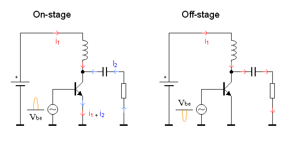
First lets have a look at the schematic. To the base of the transistor is a AC-generator connected. This signal will make the transistor conduct during the positive period. A coil is connected from power supply to the collector and there is a capacitor connected to a resistor. The capacitor at the collector remove the DC voltage and the resistor is simulating the antenna. During the positiv period of the input signal (On stage) During the positiv period of the input signal the transistor will conduct (On-state). You can imagin that the transistor is a switch which connects the emitter with the collector. What will happend now is that the current I1 (red) flow through the coil and then into the transistor and down to ground. A magnetic field builds up in the coil depending on the magnitude of the current. At the same time the voltage over the capacitor discharge through the resistor making another current flow I2 (blue) also through the transistor. The I2 current passes the resistor (antenna) which radiate the energy. During the negativ period of the input signal (Off stage) During the negativ period of the input signal the transistor will not conduct (Off-state). You can imagin that the transistor is an open switch. No current can pass through the collector to the emitter. The magnetic filed which was build upp in the coil will now collaps and generate a current I1 (red) which will flow through the capacitor and into the resistor (antenna). Input filter (impedance match) Since most most RF equipment (input/output) are matched to 50 ohm, we will try to match the input impedance of our power amplifier also to 50 ohm. The impedance from the base to emitter in the transistor is very low, 3-10 ohm depending on the transistor you are using. As you might understand, it wouldn't be a great idea to connect a RF driver made for 50 ohm to our 3-10 ohm power transmitter. The driver would probably give you a small pyrotecnical show, which could wait until new years eve. What we want is to match the impedance in the input stage so we can drive it with 50 ohm and transform all the input energy into the transistor base-emitter which is still 3-10 ohm. There are several ways to do this. One is to use a transformer with different turns of winding or like in this construction, we will use two variable capacitor and a coil to find the best match. Schematic of Input stage
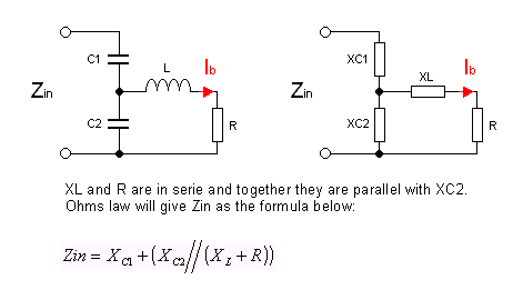
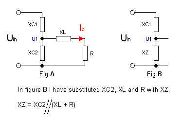
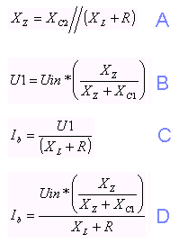
The fig above show the input stage to the transistor. Zin is the input impedance of this power amplifier. We want it to be 50 ohm so it will match the output from a previous drive stage. C1 and C2 is tunable capacitor and the resistor R in this shematic represent the input impedance of the transistor between the base and the emitter. A serie coil (L) is inserted between the base and the two capacitor. The two capacitor and the coil will transform the 50 ohm input to the 3-10 ohm impedance of the transistor and all input energy will end up in the transistor. The current Ib is the current into the base of the transistor. What do I want to find out? I want to know the values of C1, C2 and L so the impedance will be 50 ohm and to get maximum current Ib. To achieve this I need to find some mathematical formula. To make the calculations more simple I transform the capacitors and the inductor to reactances. You can see this in the right schematic. As you probably can see, the XL and R are in serie, and together they are in parallel with XC2. The formula at the bottom of the figure is the expresion of the impedans Zin. To simplify the branch with the XL and R parallel with XC2, I substitute them with an impedance called XZ.(See left fig below). Substitut XL, R and XC2 Formula calculation |
|
|
|
Contact email: qooljaq@qooljaq.com |